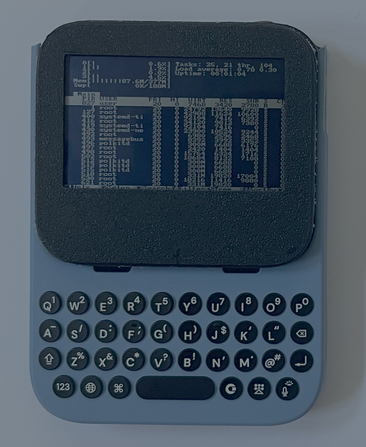
I don’t organize my things well. I try to, but quite often end up with a bunch of stuff on my desk. From various aliexpress orders and projects I’m working on, all the way to gifts and stuff I didn’t have time to find a place for.
That is exactly how this project came to be. At one point in time I had, lying on my desk:
And of course, my caveman brain combined the 3.
Okay, okay, not to lie I was probably a bit conditioned by knowing about:
Due to the mysterious laws of supply and demand, and the magic of supply chains - somehow you can get a 4G modem with WiFi, bluetooth, a display, fully battery powered and completely unlocked - for less than $20 shipped. This, of course, is the cornerstone of our project.
There are versions with and without a display. The non-display one just swaps the display for LED-s, though the PCB is the same. Display is a GC9107 powered one, but it looks like ass so i ditched it.
Linux can be installed trivially, powered by the wonderful openstick project. The stock device runs Android, but adb is accessible out of the box - and from adb you can go straight to edl and reflash the thing. Just make sure to save all the important partitions. There are also pins on the pcb which you can short out to get straight to edl.
Extracting the running device tree from the running android was a goldmine of information so be sure to do that.
Here are a few guides or links I found helpful:
The real pain with openstick starts once you get to the drivers and device trees, but we will talk about that later.
There is not much to say about the Clicks Keyboard. It feels veeery nice to use, the only issue is you need to fork over quite a few clams - made worse because you are going to have to cut it 😱.
Regarding the protocol, it’s exactly what I expected with my previous experience of working with MFi devices - just a regular USB keyboard with an additional Apple proprietary endpoint which the iPhone can authorize with before allowing the keyboard to go through.
So for our device this means that it’s just a regular keyboard.
On a side note, there is a Clicks mobile app used for configuration/updates/whatever. The keyboard itself is powered by CH32V203 or similar. Custom code could be flashed but I don’t see any reason to to this currently. In the future I would like to have a configuration utility.
I think the sharp display look great with the high contrast (and it plays well into my use case of a dumb device used only for messaging). Other than that, if there wasn’t much to say about the keyboard - then there is absolutely nothing more to say here.
It’s a display.
You send commands.
It displays.
One thing became clear to me quite fast - I was going to have to add a custom PCB. I wasn’t exactly sure what the MF800 had on-board, and I never did end up opening the shield can - but I am fairly certain there is no 5V booster on-board.
Because of the physical sizes, which we will go over further in the post, the USB connector will end up chopped off - so we need a way to handle that too.
The final PCB ended up handling the USB host mode power, USB host/device mode switching, display power and display signal level conversion.
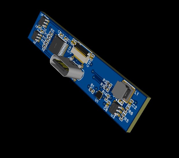
I ordered the PCB along with assembly. And because 2 sided assembly is expensive, I made a few compromises to fit all the components on one side. The non-component side is used for the solder points for the PCB-to-PCB connections.
All files can be found on GitHub, but in short the PCB consists of:
The MF800 is quite a bit bigger than other opensticks, partly because of the battery it has to include, partly because of it’s slop nature.
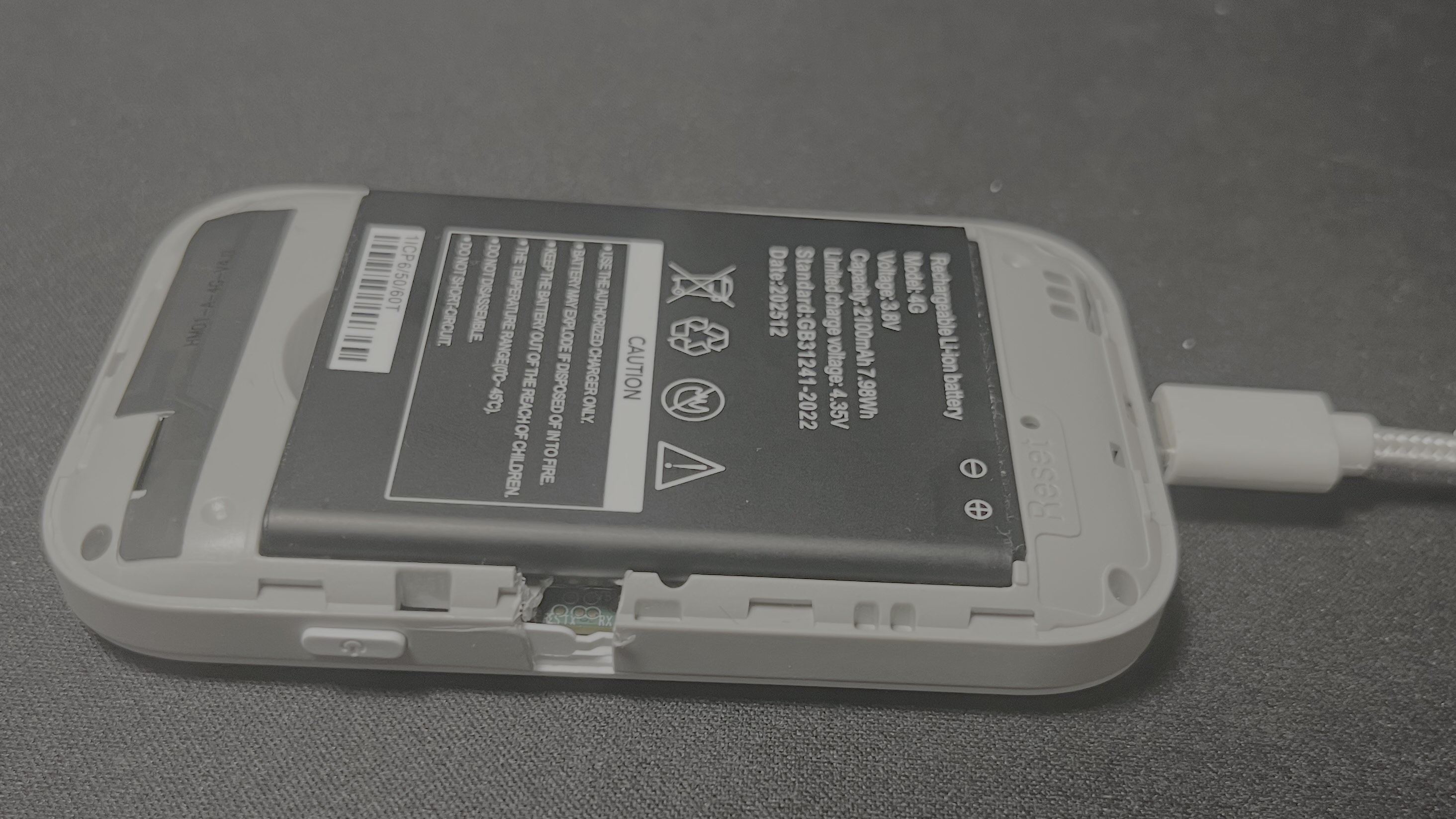
So to fit inside a Clicks case, we either orient it verticaly and and up with a humongous abomination, or we trim the pcb to fit horizontally.
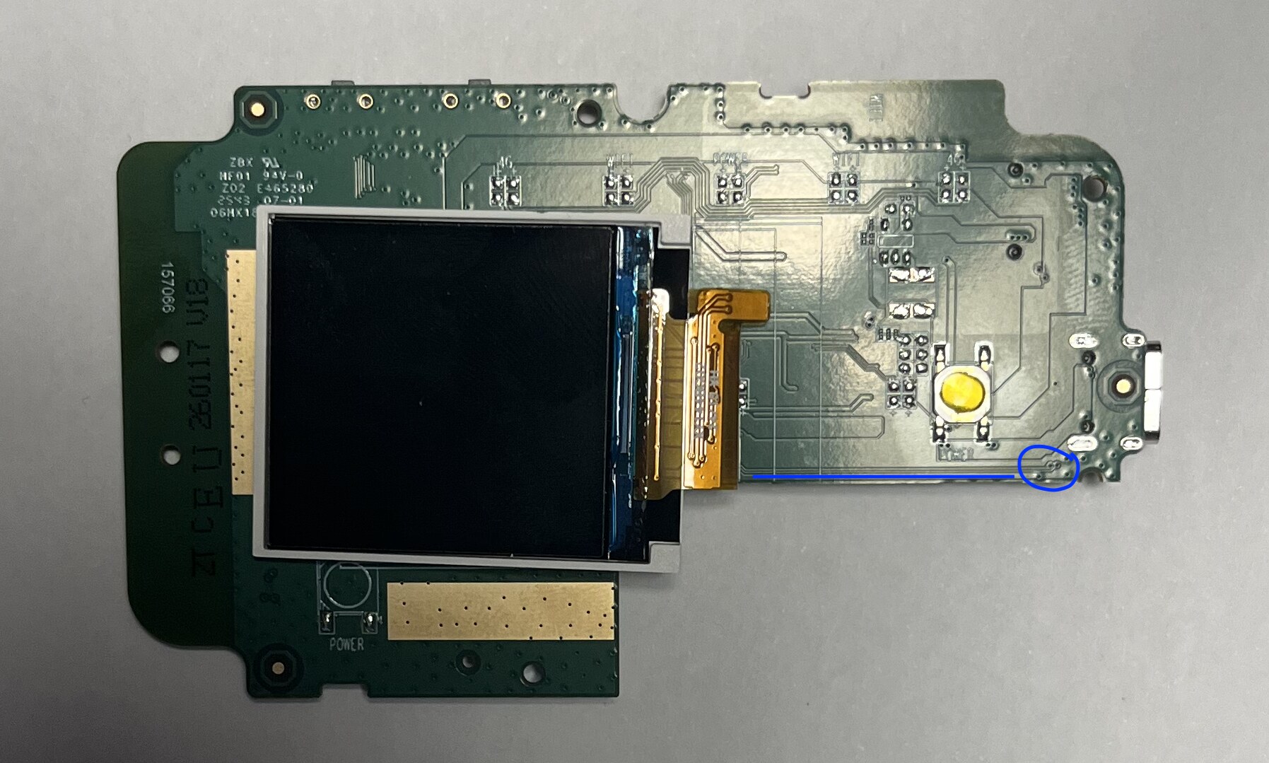
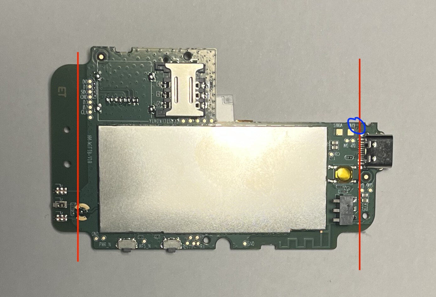
Notice that my right cut (on the bottom picture) cuts off the battery connection line, so this will have to be patched up later.
Cutting the PCB went unexpectedly well. The device booted up immediately and everything seemed to work. Turns out there really were no crucial lines going through those areas of the PCB.
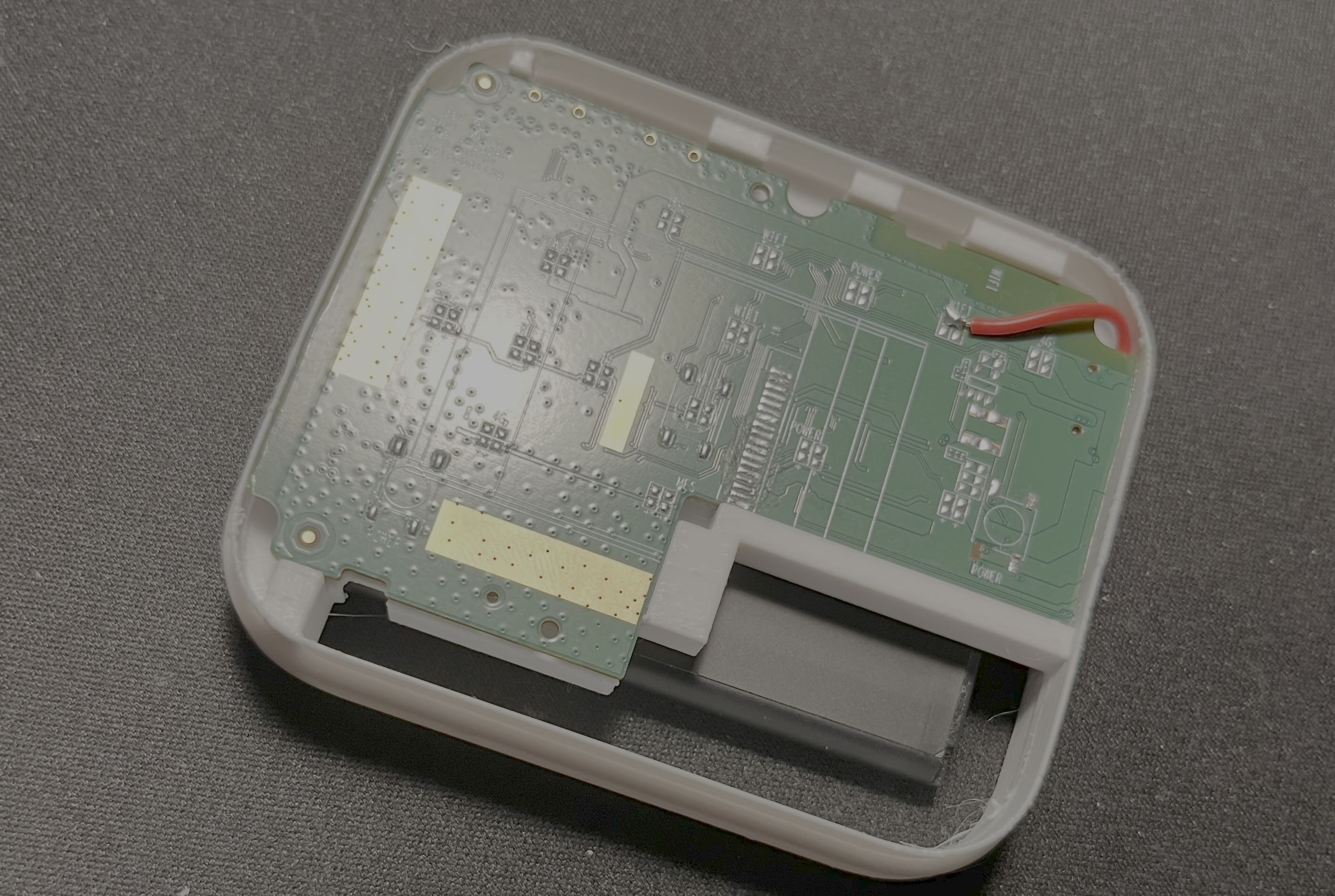
Only things I didn’t test were the USB connection and the 4G modem. The modem I was 99% sure wouldn’t be an issue as there is no reason to route anything for it under those areas - but regarding the USB I was worried that I hadn’t maybe nicked the via.
I decided to reuse the pads from the old display. I don’t really know why anymore - possibly because my initial ideas was to use a rigid flex PCB and solder it similar to how the original display was. (which I decided against immediately upon seeing the prices)
Looking at all this now, it seems very dumb. I should have used the labeled pads next to the unpopulated micro SD connector. Note that never did check if these were shared with the SIM card though.
Since I could boot the device and I had the original android device
trees, I extracted which pins were used for the display SPI. I then
tested those with gpioset to make sure that I was indeed
correct. Same goes for the power supplies (although I tested those by
disabling them in the device tree and rebooting) and grounds.
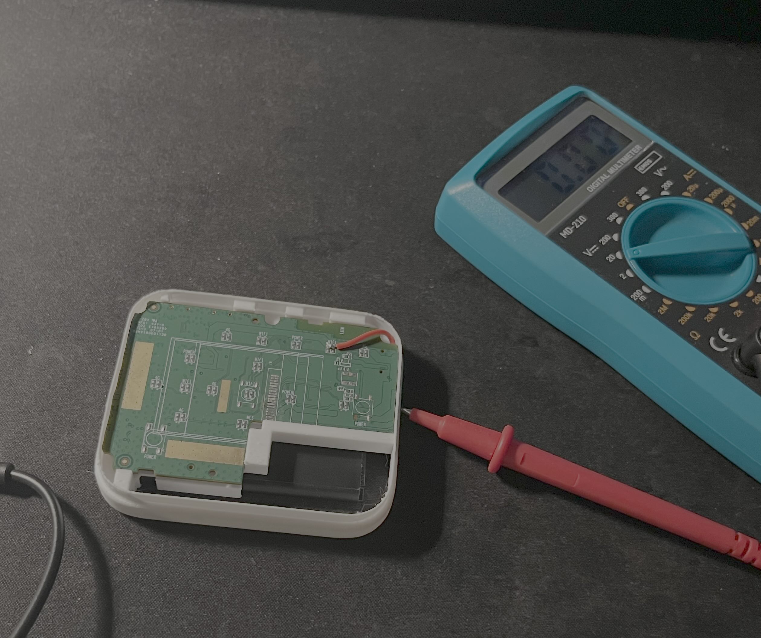
The first thing I wired and checked were the power supplies followed by the USB. This is because I could test this as an isolated unit. I was also more skeptical about this because it involved a bit of circuitry on my part as well as that iffy via.
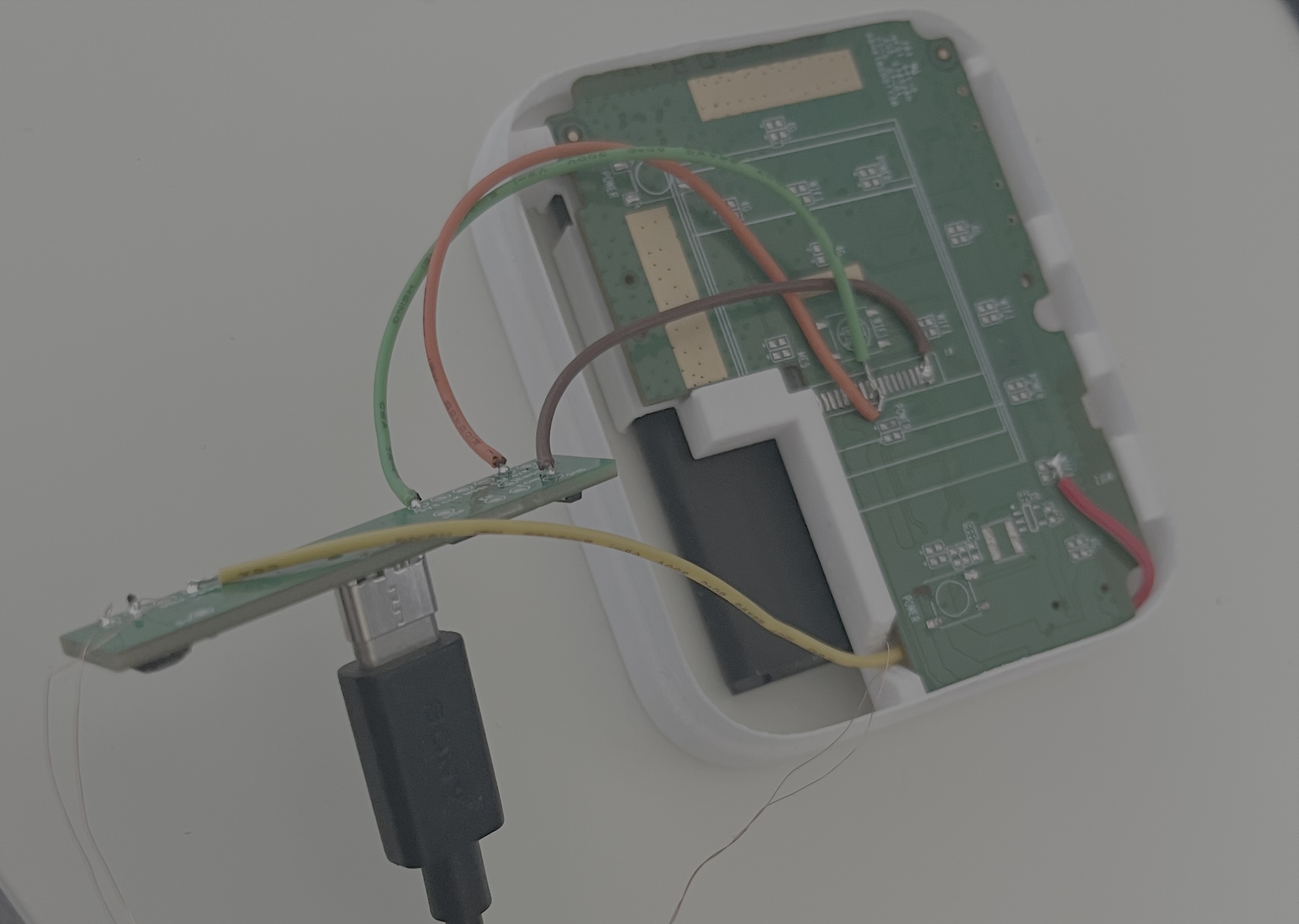
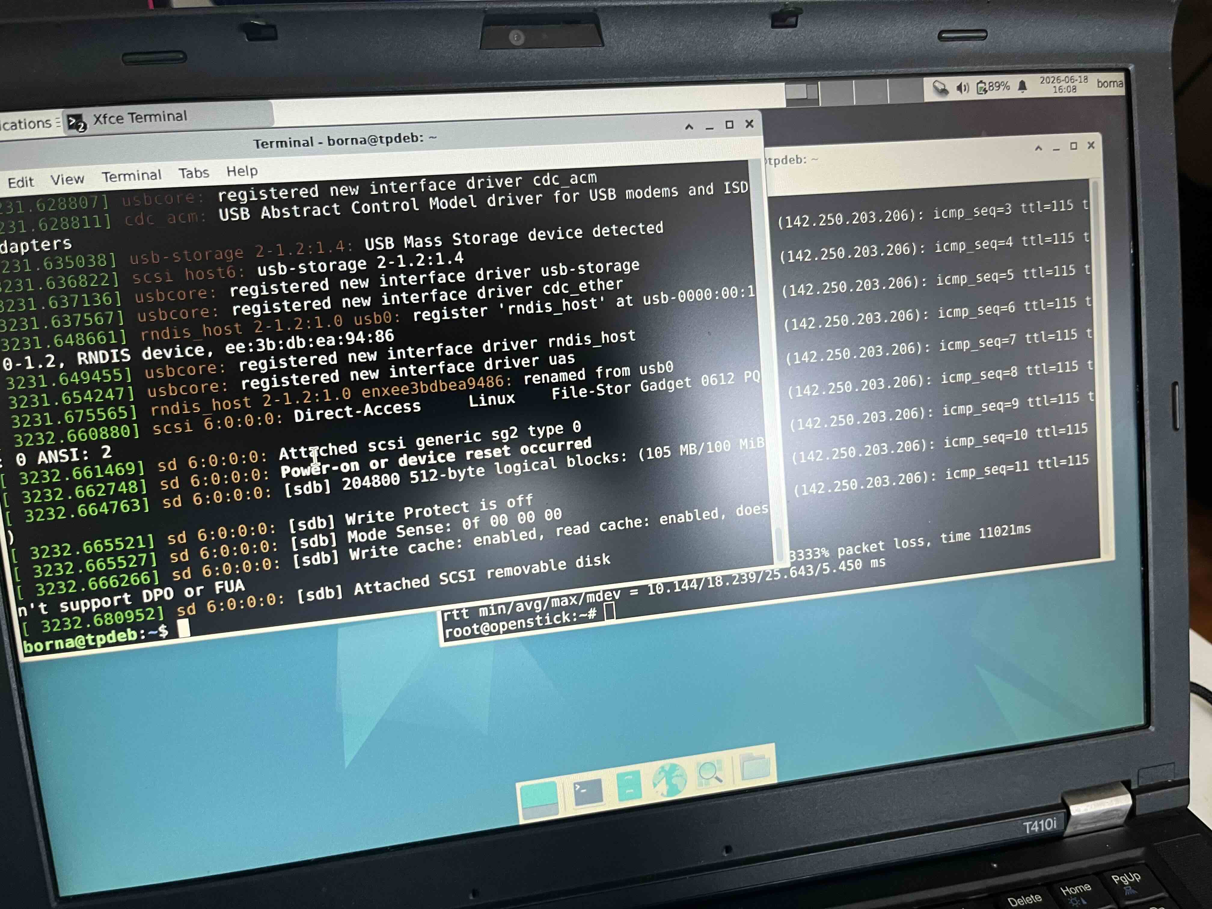
Of course, it didn’t work initially. After probing around the pads
and seeing that all the voltages were OK I noticed in my laptop’s
dmesg that it TRIED to enumerate - meaning something was
going on.
I also noticed that it says "high-speed". This caught me a bit off guard. I didn’t expect it to use "high-speed" USB. My first thought was that the wires were too long. But before shortening them, I tried a quick fix - twisting them more tightly - and it worked 😲!
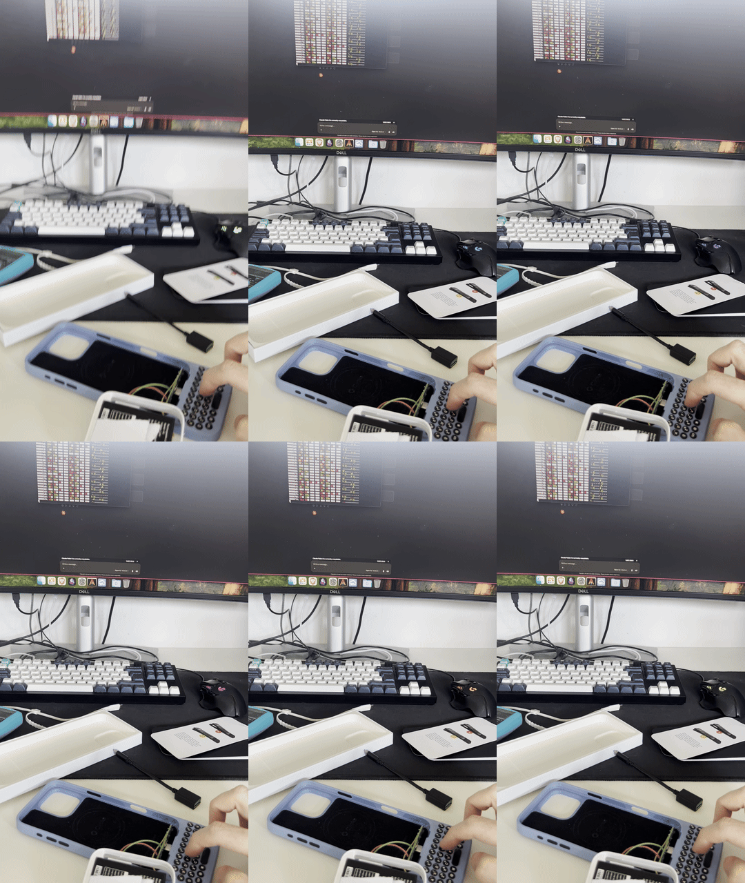
Immediately following this success, I tried to get the other direction working. This took some time. Turns out, not all aliexpress adapters correctly wire the CC lines. The keyboard did work immediately, though - only issue is I was afraid to test with it first in case something was wired incorrectly.
Before wiring the SPI lines to the display, I wanted to check if I had correctly reconfigured my device tree. I knew the pads were correct from the earlier testing, but there is quite a lot which can go wrong here.
spi@78b9000 {
    compatible = "qcom,spi-qup-v2.2.1";
    reg = <0x78b9000 0x500>;
    interrupts = <0x00 0x63 0x04>;
    clocks = <0x13 0x41 0x13 0x36>;
    clock-names = "core", "iface";
    dmas = <0x6d 0x0c 0x6d 0x0d>;
    dma-names = "tx", "rx";
    pinctrl-names = "default", "sleep";
    pinctrl-0 = <0x84>;
    pinctrl-1 = <0x85>;
    #address-cells = <0x01>;
    #size-cells = <0x00>;
    status = "okay";
    spidev@0 {
        //compatible = "linux,spidev";
        compatible = "rohm,dh2228fv";
        reg = <0>;
        spi-max-frequency = <16000000>;
        spi-cs-high;
    };
};
For example, qualcomm drivers are sketchy and the commented out
compatible won’t actually export the spidev, so we scam it
with this the dh2228fv compatibility.
Using the spi-pipe utility running in a loop, I was able
to measure voltage change on the MOSI and CLK lines - which was enough
for me to conclude that something was happening. I would, of course,
prefer to do this with a scope or a logic analyzer - but I didn’t have
any of those at hand.
Encouraged by the major success of power supplies and USB, I carelessly connected the display into the PCB (while the device was on 🤦).
Immediately something happened to the display and I was sure I broke it. Fortunately nothing came of this and the display was fine. (This actually happens every time I turn on the device. I don’t yet know if I should be concerned 😬.)
Once I reassured myself that nothing bad had happened, and that nothing was smoking or overheating - I proceeded with trying to get the display to work.
After an hour of slopping through this with AI python code I was absolutely nowhere. There were multiple possible points of failure. Level converter, bad routing, contacts, etc…
Turns out, as is quite common (IDK why), the qualcomm driver doesn’t
handle the CS well (or correctly - or maybe it does but for other use
cases). In any case, I tried again the same test script, but this time
toggling the CS pin manually (via libgpiod) - and it
actually worked.
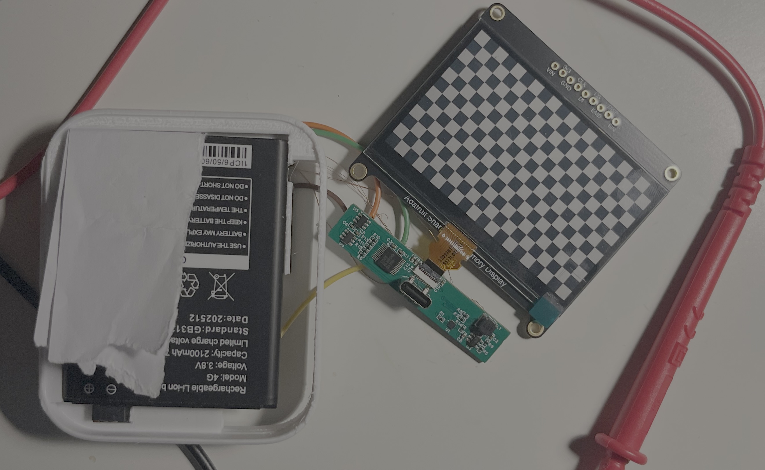
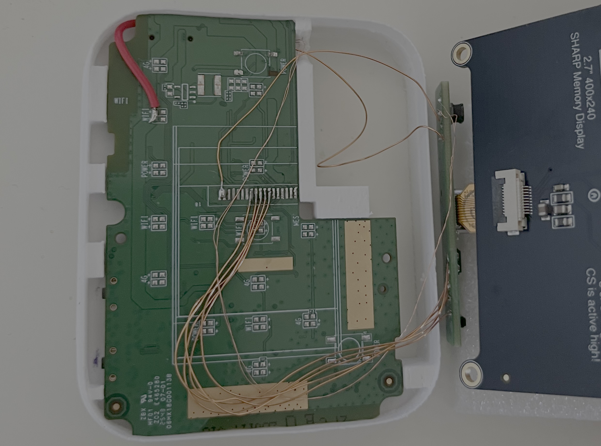
I was immediately dissapointed with the everything. From the "electrical" wire I used to connect the power supplies to the sketchy tiny magnet wire I used for the signals all the way to the twisted ground I wrapped around MOSI and CLK (which seemed to do nothing) - so I decided to rewire everything once more.
This time i used magnet wire for both signals and power, but this one was quite a bit thicker and also kept position once bent. I didn’t rewire the USB data lines though, as the pads on the main board look very iffy.
All the previous tests were done with just dumb python scripts, but
the real way forward is with a kernel driver. There are quite a few
drivers available, but the one I picked is ardangelo’s
sharp-drm-driver. My reasons for wanting a DRM driver
are as follows:
mpv)
This worked almost immediately. I did have to playing around with CS and it’s active high default.
For probably the first time in my life I didn’t have any issues
compiling the kernel module and running it. The mystery kernel I was
running was a 6.12.1-msm8916 one with modules enabled. It
had a .config file present which I took.
Next I downloaded the mainline linux 6.12.1 kernel and
hoped that there weren’t any (or significant) changes. This ended up
being enough, and after a few small patches to the driver the thing just
worked.
Below is what the device tree ended up looking like. Notice that the CS logic being handled by the display driver.
spi@78b9000 {
    compatible = "qcom,spi-qup-v2.2.1";
    reg = <0x78b9000 0x500>;
    interrupts = <0x00 0x63 0x04>;
    clocks = <0x13 0x41 0x13 0x36>;
    clock-names = "core", "iface";
    dmas = <0x6d 0x0c 0x6d 0x0d>;
    dma-names = "tx", "rx";
    pinctrl-names = "default", "sleep";
    pinctrl-0 = <0x84>;
    pinctrl-1 = <0x85>;
    #address-cells = <0x01>;
    #size-cells = <0x00>;
    status = "okay";

    sharp_drm@0 {
        compatible = "sharp-drm";
        reg = <0>;
        spi-max-frequency = <4000000>;
        cs-gpios = <0x49 18 1>;
    };
};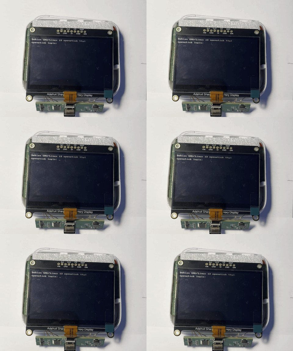
Issue now is that the driver just rounds pixel color under some value to black, above that to white (or inverted, depends on parameters). For text (or if you do the visuals yourself in your app) this works great - but for a general purpose solution where you want to play videos or show images - this looks like ass. The fix for this is to add dithering to the driver.
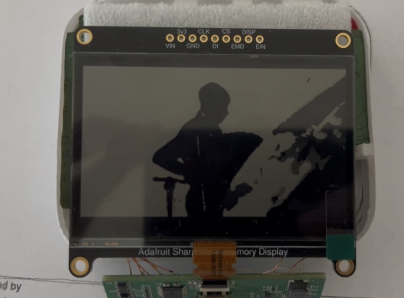
I added a custom sys value which allows the user to enable dithering, as well as to pick which algorithm they want:
All the initial functionality was left intact.
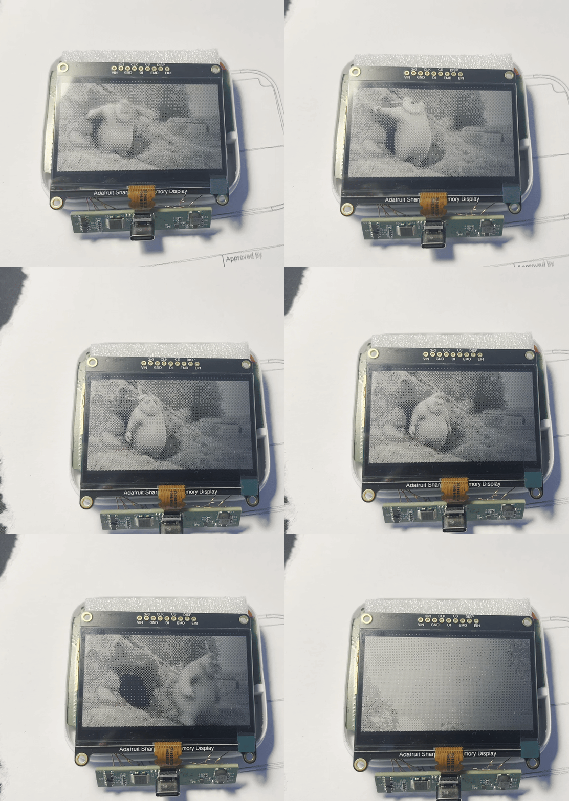
You can find more information about this, or the DRM driver patches on the project’s GitHub repo.
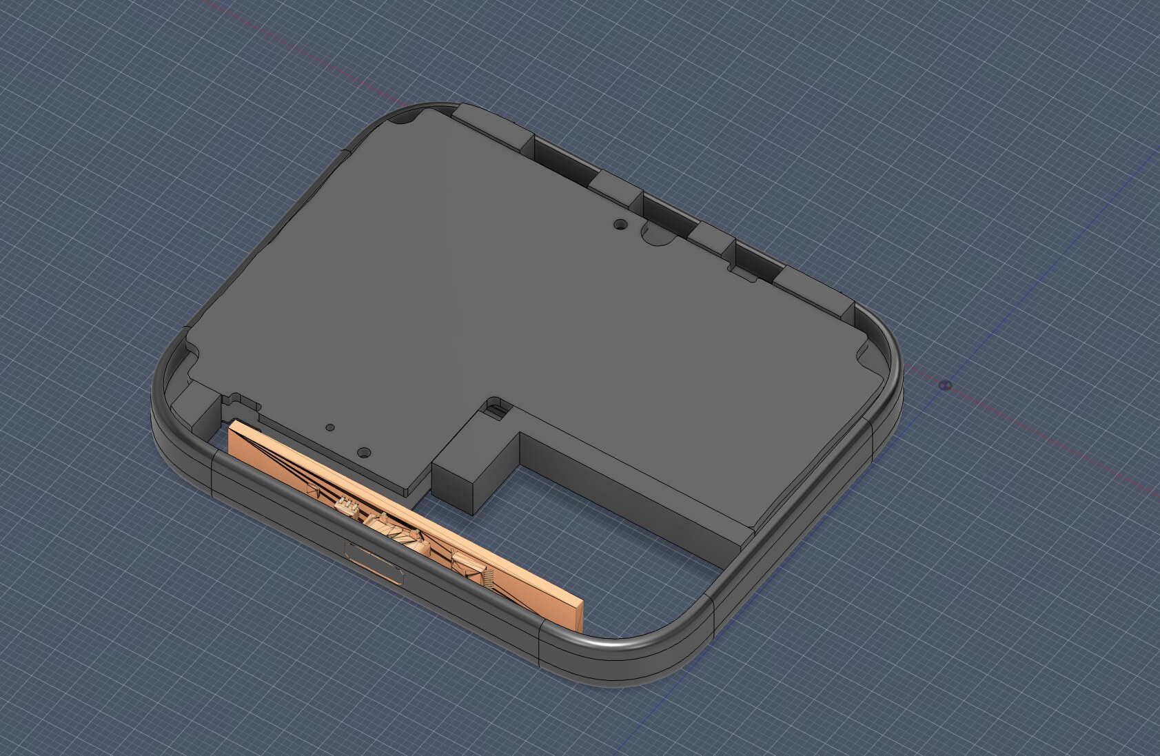
With everything on my table and working, mainly meaning the dimensions are set and can be measured, I jumped into modeling the near-final case which I can hopefully put into the keyboard case without worrying about breaking anything.
This was kinda sketchy since apple doesn’t give dimensions of how far the USB-C connector is inside the iPhone - but I got around this by measuring apple standard USB-C cables (which fit snug up to the device) and interpolating from there.
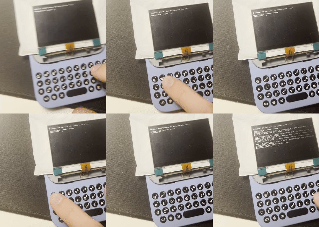
This print still wasn’t particullarly useful but served it’s purpose to confirm that the USB connector dimensions (among others) were measured correctly.
Also, 2 sidewalls didn’t print correctly and while modelling (this was before I receive’d one visible in the pictures) I didn’t have a display (except the one bonded to the devkit PCB) to model off of, so the cover is lacking.
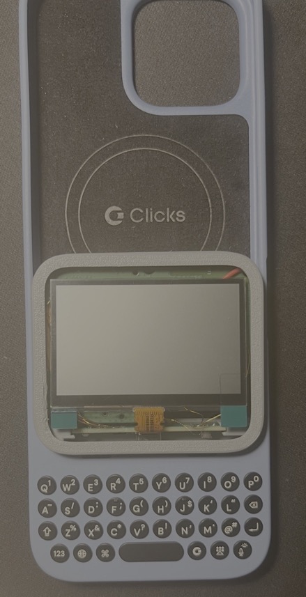
This is what ended up being the final enclosure. Mostly everything fit correctly. I first whipped up a quick test held together by kapton tape.
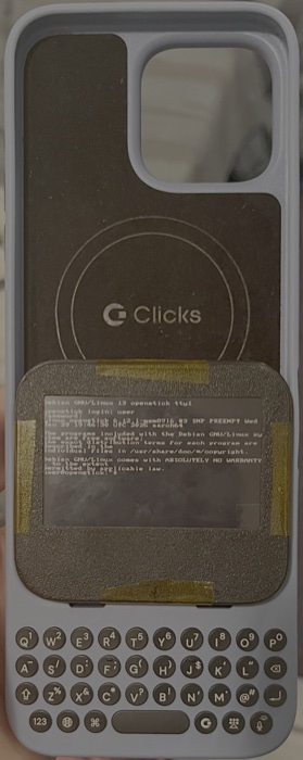
This was the point at which, becuase of some ongoing life stuff, I temporarily lost access to a big chunk of my tools (mainly the 3D printer but also other stuff).
My hand being forced, I decided to hot glue the case together instead of printing a final final one which clips together.
I also forgot about the power button, which despite being on the PCB and working - didn’t get a case cutout and a plunger. This was solved with a small hole and a pin. Very ugly but it works.
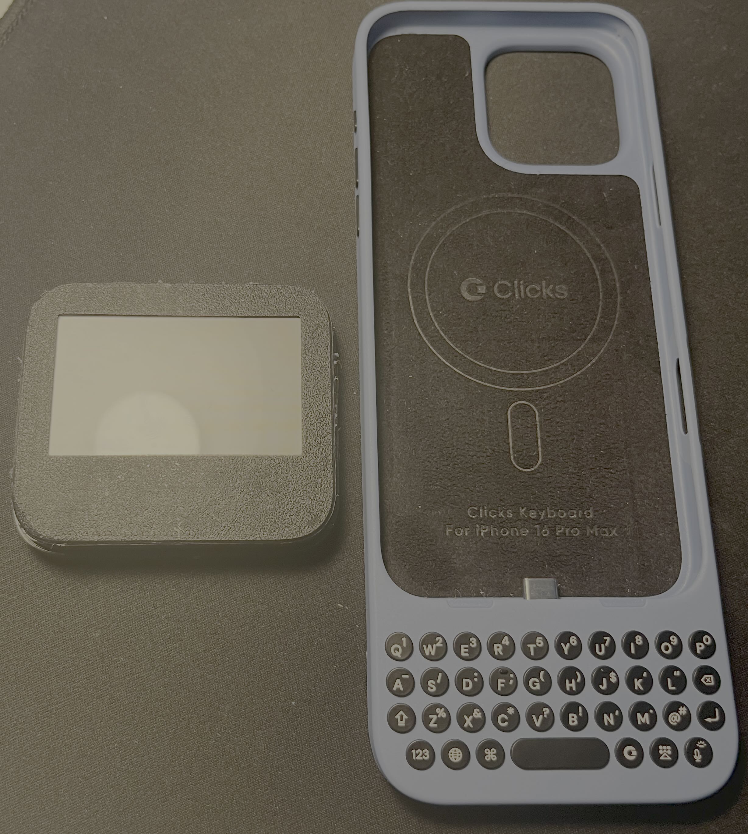
Now the big boy moment - cutting down the keyboard case with no tools. It went about as well as you can expect. Though I made sure to cut less than needed so that I can sand it down and make it look pretty once I get my gear back.
It realistically doesn’t look that bad, but the edges could use some cleaning. The case hot glue protrusion is a bigger issue.
With the magic of top-down photos I have hidden most of this from you.
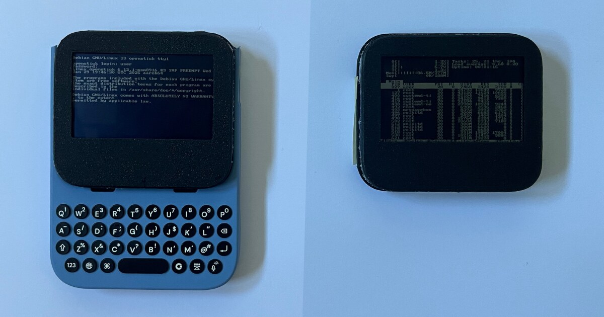
I forgot to take photos while assembling this. It’s exactly the same as before plus a 4G flex PCB antenna which I soldered to the PCB and glued below the display on the top half of the enclosure. There is now also a mini SIM in it’s slot.
The android device trees I copied from the device come predefined with the battery and charger configurations. These are also more advanced than the ones offered by the mainline linux i’m running.
Still, I expected it to be pretty easy to get something usable working. Big questions here were the battery information and power draw of my adapter PCB.
What the driver provided on the user level, however, was only the battery voltage in uV and a flag whether it’s charging or not. So the actual battery logic will be left up to my app as I’m not planning to mod the driver just for the battery percent value.
Charging seems to work fine. It also works via the keyboard USB passthrough port, but unfortunately only when the device is booted up.
Sleep currently stands as the biggest non-solved issue. Main reason is the lack of day-to-day testing of the device, especially with the modem turned on - and the lack of a convenient power button.
I’m planning to tackle this in the near future as I begin using the device for my messaging. I would like to get a fast bootup/shutdown going on at the very least.
Additional input methods, eg. a touch screen or a scroll wheel, would probably be the best additional feature. Touch, especially, can be done with very little space.
Those are followed closely by sound or vibration. Even a tiny speaker at like 8khz. There is sufficient PCB space for an amplifier as well as space for the speaker in the enclosure.
Mainly the glue issue and the missing power button, both of which require a new print, plus the jagged edges on the keyboard case that need filing down.
The battery is held down by a bit of tape as it otherwise falls out when not in the case. Not a priority at the moment.
The big bottom bezel driving the enclosure height could also be shortened, but that would require sourcing a different battery with the same 3 pin connector among other things.
The helper PCB slides up inside it’s slot because the display FPC cable slightly pulls on it and I forgot to add tabs in the enclosure cover to keep it in place. Not ideal - but it’s only an issue when sliding the enclosure into the case.
Finally, a tiny portion of the display is covered by the case. Like 1-2 pixels on all edges. This will also be fixed with the next print.
All in all I’m very happy with the device, but a bit more work would do wonders for the visuals. In photos it looks fine - in real life it leaves a little to be desired.
If you are interested in replicating this or doing something similar, you can find most of the stuff on the project’s GitHub repo.
I have deliberately omitted software from this post since that will only get ironed out with use, and I’m not a big fan of releasing projects I haven’t finished but didn’t drop.
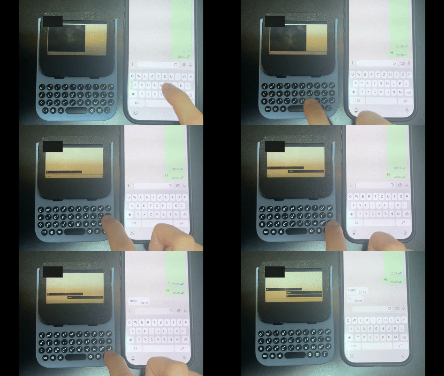
As of writing this I already found a memory leak in the original display driver. I also shipped a patch which fixes it. Stuff like this can’t easily be found without actual hands-on testing.
The text was fully written by me, a human.
You can contact me at veggie_privacy_8y at icloud dot com